Easy Way to Explain 110 of 003
A Full-wave rectifier is a circuit arrangement that makes use of both half cycles of input alternating current (AC) and converts them to direct current (DC). In our tutorial on Half-wave rectifiers , we have seen that a half-wave rectifier makes use of only one-half cycle of the input alternating current. Thus a full-wave rectifier is much more efficient (double+) than a half-wave rectifier. This process of converting both half cycles of the input supply (alternating current) to direct current (DC) is termed full-wave rectification.
The full-wave rectifier can be constructed in 2 ways. The first method makes use of a centre tapped transformer and 2 diodes. This arrangement is known as Center Tapped Full-Wave Rectifier .
The second method uses a normal transformer with 4 diodes arranged as a bridge. This arrangement is known as a Bridge Rectifier.
Full Wave Rectifier Theory
To understand full wave bridge rectifier theory perfectly, you need to learn half wave rectifier first. In the tutorial on the half-wave rectifier, we have clearly explained the basic working of a rectifier. In addition, we have also explained the theory behind a p-n junction and the characteristics of a p-n junction diode .
Full Wave Rectifier – Working & Operation
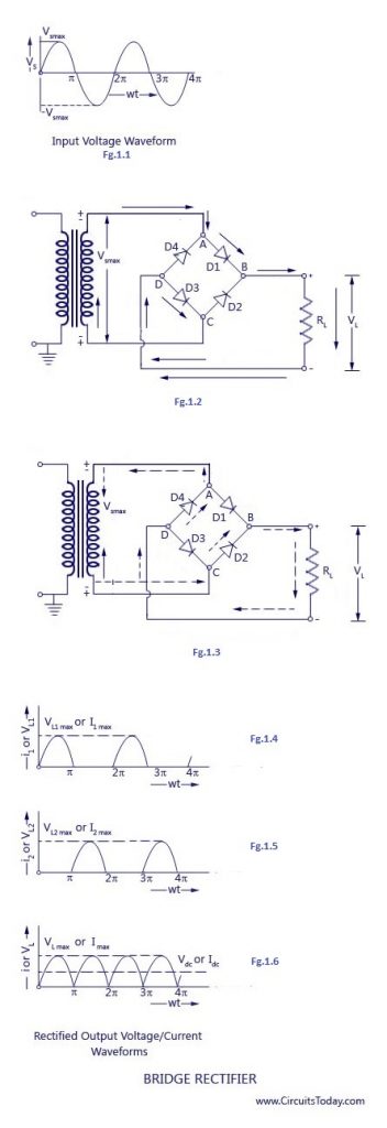
The working & operation of a full-wave bridge rectifier is pretty simple. The circuit diagrams and waveforms we have given below will help you understand the operation of a bridge rectifier perfectly. In the circuit diagram, 4 diodes are arranged in the form of a bridge. The transformer secondary is connected to two diametrically opposite points of the bridge at points A & C. The load resistance RL is connected to the bridge through points B and D.
During the first half cycle
During the first half cycle of the input voltage, the upper end of the transformer secondary winding is positive with respect to the lower end. Thus during the first half cycle, diodes D1 and D3 are forward biased and current flows through arm AB enters the load resistance RL, and returns back flowing through arm DC. During this half of each input cycle, the diodes D2 and D4 are reverse biased and current is not allowed to flow in arms AD and BC. The flow of current is indicated by solid arrows in figure 1.2 above. We have developed another diagram below to help you understand the current flow quickly. See the diagram below – the green arrows indicate the beginning of current flow from the source (transformer secondary) to the load resistance. The red arrows indicate the return path of current from load resistance to the source, thus completing the circuit.

During the second half cycle
During the second half cycle of the input voltage, the lower end of the transformer secondary winding is positive with respect to the upper end. Thus diodes D2 and D4 become forward biased and current flows through arm CB, enters the load resistance RL, and returns back to the source flowing through arm DA. The flow of current has been shown by dotted arrows in figure 1.3. Thus the direction of flow of current through the load resistance RL remains the same during both half cycles of the input supply voltage. See the diagram below – the green arrows indicate the beginning of current flow from the source (transformer secondary) to the load resistance. The red arrows indicate the return path of current from load resistance to the source, thus completing the circuit.

Peak Inverse Voltage of a Full wave bridge rectifier:
Let's analyse the peak inverse voltage (PIV) of a full-wave bridge rectifier using the circuit diagram. At any instant when the transformer secondary voltage attains positive peak value Vmax, diodes D1 and D3 will be forward biased (conducting) and the diodes D2 and D4 will be reverse biased (non conducting). If we consider ideal diodes in the bridge, the forward biased diodes D1 and D3 will have zero resistance. This means voltage drop across the conducting diodes will be zero. This will result in the entire transformer secondary voltage being developed across the load resistance RL.
Thus PIV of a bridge rectifier = Vmax (max of secondary voltage)
Bridge Rectifier Circuit Analysis
The only difference in the analysis between full wave and centre tap rectifier is that
- In a bridge rectifier circuit, two diodes conduct during each half cycle and the forward resistance becomes double (2R F ).
- In a bridge rectifier circuit, Vsmax is the maximum voltage across the transformer secondary winding whereas in a centre tap rectifier Vsmax represents that maximum voltage across each half of the secondary winding.
The different parameters are explained with equations below:
-
Peak Current
The instantaneous value of the voltage applied to the rectifier is given as
vs = Vsmax Sin wt
If the diode is assumed to have a forward resistance of R F ohms and a reverse resistance equal to infinity, the current flowing through the load resistance is given as
i1 = Imax Sin wt and i2 = 0 for the first half cycle
and i1 = 0 and i2 = Imax Sin wt for second half cycle
The total current flowing through the load resistance R L, being the sum of currents i1 and i2 is given as
i = i1 + i2 = Imax Sin wt for the whole cycle.
Where the peak value of the current flowing through the load resistance R L is given as
Imax = Vsmax/(2R F + R L )
2. Output Current
Since the current is the same through the load resistance RL in the two halves of the ac cycle, the magnitude of dc current Idc, which is equal to the average value of ac current, can be obtained by integrating the current i1 between 0 and pi or current i2 between pi and 2pi.

3. DC Output Voltage
The average or dc value of voltage across the load is given as

4. Root Mean Square (RMS) Value of Current
RMS or effective value of current flowing through the load resistance R L is given as

5. Root Mean Square (RMS) Value of Output Voltage
RMS value of voltage across the load is given as

6. Rectification Efficiency
Power delivered to load,

7. Ripple Factor
The form factor of the rectified output voltage of a full-wave rectifier is given as

So, ripple factor, γ = 1.11 2 – 1) = 0.482
8. Regulation
The dc output voltage is given as

Merits and Demerits of Full-wave Rectifier Over Half-Wave Rectifier
Merits – let us talk about the advantages of a full-wave bridge rectifier over a half-wave version first. I can think about 3 specific merits at this point.
- Efficiency is double for a full-wave bridge rectifier. The reason is that a half-wave rectifier makes use of only one half of the input signal. A bridge rectifier makes use of both halves and hence double efficiency
- The residual ac ripples (before filtering) are very low in the output of a bridge rectifier. The same ripple percentage is very high in a half-wave rectifier. A simple filter is enough to get a constant dc voltage from the bridge rectifier.
- We know the efficiency of the full-wave rectifier is double than the half-wave rectifier. This means higher output voltage, Higher transformer utilization factor (TUF) and higher output power.
Demerits – Full-wave rectifier needs more circuit elements and is costlier.
Merits and Demerits of Bridge Rectifier Over Center-Tap Rectifier.
A centre tap rectifier is always a difficult one to implement because of the special transformer involved. A centre tapped transformer is costly as well. One key difference between centre tap & bridge rectifier is in the number of diodes involved in construction. A centre tap full wave rectifier needs only 2 diodes whereas a bridge rectifier needs 4 diodes. But silicon diodes being cheaper than a centre tap transformer, a bridge rectifier is a much-preferred solution in a DC power supply. Following are the advantages of a bridge rectifier over a centre tap rectifier.
- A bridge rectifier can be constructed with or without a transformer. If a transformer is involved, any ordinary step-down/step-up transformer will do the job. This luxury is not available in a centre tap rectifier. Here the design of the rectifier is dependent on the centre tap transformer, which can not be replaced.
- The bridge rectifier is suited for high voltage applications. The reason is the high peak inverse voltage (PIV) of the bridge rectifier when compared to the PIV of a centre tap rectifier.
- The transformer utilization factor (TUF) is higher for the bridge rectifiers.
Demerits of Bridge rectifier over centre tap rectifier
The significant disadvantage of a bridge rectifier over a centre tap is the involvement of 4 diodes in the construction of the bridge rectifier. In a bridge rectifier, 2 diodes conduct simultaneously on a half cycle of input. A centre tap rectifier has only 1 diode conducting on a one-half cycle. This increases the net voltage drop across diodes in a bridge rectifier (it is double the value of the centre tap).
Applications of Full-wave Bridge rectifier
Full-wave rectifier finds uses in the construction of constant dc voltage power supplies, especially in general power supplies. A bridge rectifier with an efficient filter is ideal for any type of general power supply applications like charging a battery, powering a dc device (like a motor, led etc) etc. However, for an audio application, a general power supply may not be enough. This is because of the residual ripple factor in a bridge rectifier. There are limitations to filtering ripples. For audio applications, specially built power supplies (using IC regulators) may be ideal.
Full-Wave Bridge Rectifier with Capacitor Filter
The output voltage of the full-wave rectifier is not constant, it is always pulsating. But this cannot be used in real-life applications. In other words, we desire a DC power supply with a constant output voltage. In order to achieve a smooth and constant voltage, a filter with a capacitor or an inductor is used. The circuit diagram below shows a half-wave rectifier with a capacitor filter.

Ripple factor in a bridge rectifier
The ripple factor is a ratio of the residual ac component to the dc component in the output voltage. The ripple factor in a full-wave bridge rectifier is half than that of a half-wave rectifier.
Here are some projects that are based on the full-wave rectifier
- Variable lab-bench power supply
- Mobile and laptop charger
- Full-wave rectifier using SCR
- 12V power supply for LEDs strip
- Uninterruptible Power Supply (UPS)
References
- To explain the concepts better, we have referred to several textbooks, especiallyPrinciples of Electronics.
- To create the easy to understand images, we have referred to this article.
Source: https://www.circuitstoday.com/full-wave-bridge-rectifier
0 Response to "Easy Way to Explain 110 of 003"
Post a Comment